VLSIP Technologies serves as a comprehensive engineering foundry providing a full array of advanced interconnect technologies ranging from the wafer to system-level assembly. Our technical capabilities begin with turnkey design and optimization services, including schematics, layouts, frequency simulation, thermal imaging, and 3D modeling used to transition projects from concept to functional prototypes.
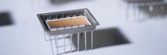
We specialize in complex assembly solutions such as flip chip, stacked die, 3D packaging, and System-in-Package (SiP), utilizing high-precision processes like eutectic die attach and various specialized bonding techniques, including ball, wedge, and ribbon bonding.
VLSIP also offers extensive wafer services, with experience handling diverse materials like SiGe, GaAs, and GaN, and capabilities for mechanical sawing, back grinding, and auto die sorting. To ensure product integrity, we provide full parametric and RF electrical testing alongside rigorous reliability qualification and failure analysis using advanced tools such as scanning acoustic microscopy (CSAM), 2D X-ray, and CT scans.
These capabilities are supported by a ubiquitous quality strategy and a tightly managed global supply base to meet the demanding requirements of the medical and defense industries.
Learn more about our technical capabilities and how VLSIP can help turn your concept into revenue.