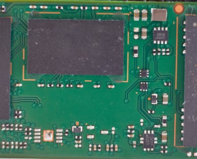
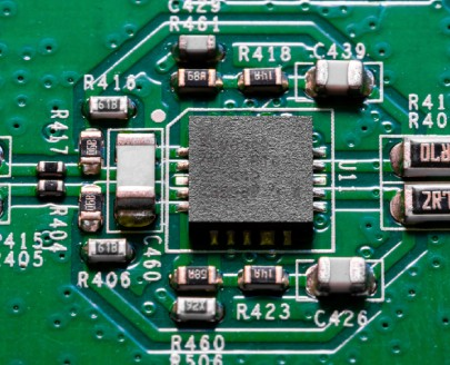
At VLSIP Technologies, we operate as an Engineering Foundry for Electronics®, providing a full array of advanced interconnect technologies that span from the wafer level to complete system-level assembly. Our core production support includes Surface Mount Technology (SMT), Circuit Card Assembly (CCA), and specialized BGA packaging, all performed within highly controlled environments.
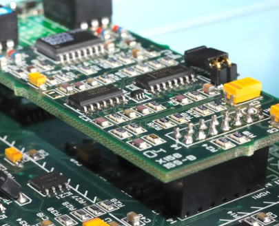
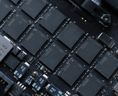
We also specialize in high-density integration through Multi-Chip Modules and sophisticated 3D Packaging solutions such as System-in-Package (SiP), Package on Package (PoP), and stacked die configurations.
By leveraging our global supply base and over 40 years of experience, we offer a Full Turnkey Engagement model that guides your product from its initial concept and circuit design through to Box Build Final Assembly.
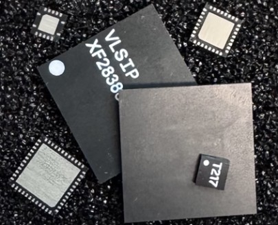
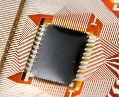
We pride ourselves on delivering breakthrough solutions for your most challenging interconnection needs through high-precision manufacturing, achieving placement accuracies of ± 3µm and bond lines within ± 0.0003”. Our technical capabilities allow VLSIP Technologies to offer highly specialized services, including LIDAR assembly for multi-laser systems, high-power electro-optics IC assemblies, and SiP die stacking on ceramic substrates as thin as 25µm.
Every project benefits from our ability to develop a custom assembly process tailored to your product, which includes meticulous material selection, custom tooling development, and automated die sorting. This expertise extends across a wide variety of wafer materials, including chips made from Si, SiGe, GaAs, GaN, GaP, InP, and AlSb, ensuring we consistently advance the technology curve of electronic module circuitry.